AMD is making a significant investment in the future of semiconductor technology with the reported establishment of a $280 million silicon photonics research and development hub in Taiwan. According to an article titled “AMD Reportedly Establishes $280 Million Silicon Photonics Hub in Taiwan; New R&D Center Could Accelerate Company’s Co-Packaged Optics Roadmap,” published by StartupNews.fyi, the new facility signals the chipmaker’s deepening commitment to next-generation optical interconnect technologies, specifically in the area of co-packaged optics.
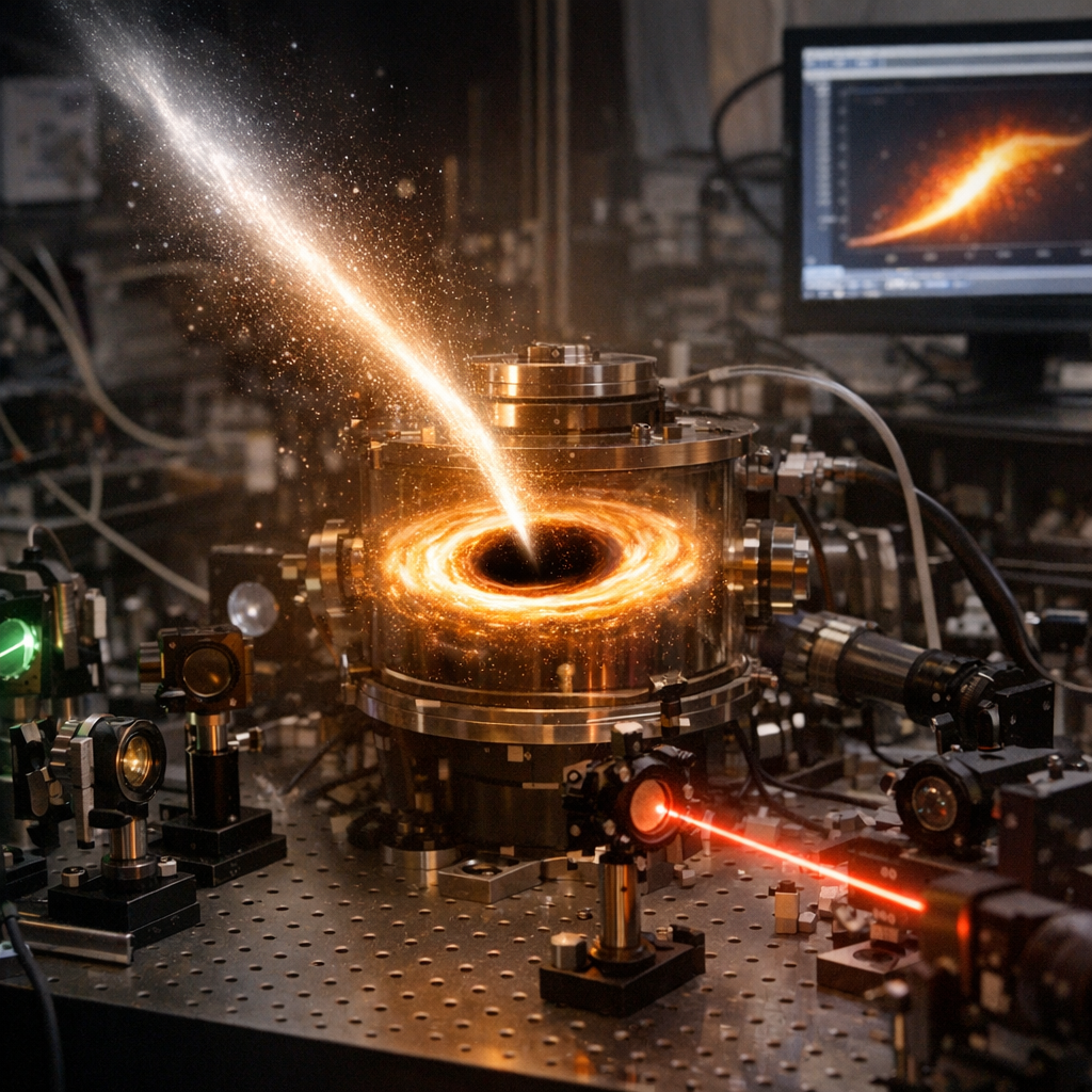
The upcoming R&D center is expected to focus on silicon photonics—a field that integrates optical components into silicon chips—to address growing data demands and performance bottlenecks in data centers, artificial intelligence applications, and high-performance computing. The shift underscores AMD’s strategic emphasis on reducing latency and power consumption in data-intensive systems by embedding optical links directly into processors, a move seen as essential for sustaining innovation in an era where traditional electrical interconnects are fast approaching their physical limits.
The Taiwan hub will not only bolster AMD’s technological capabilities but also strengthen its presence in a region that serves as a cornerstone of the global semiconductor supply chain. By situating the center in Taiwan, AMD taps into a rich ecosystem of fabrication facilities, materials suppliers, and technical expertise critical for accelerating advances in silicon photonics.
Though AMD has not formally confirmed the development, the move aligns closely with the company’s recent trajectory. Over the past several years, AMD has made targeted acquisitions and broadened its engineering capacity to keep pace with competitors like Intel and NVIDIA, both of which have been making parallel investments in optical interconnects and advanced packaging technologies. Co-packaged optics—a method of combining optical and electronic components in a single package—is widely viewed as a fundamental building block for the next wave of data infrastructure, capable of enabling significantly faster data transfer rates with lower energy requirements.
If realized as described, the new R&D hub could play a pivotal role in AMD’s long-term strategy by catalyzing innovation across its product lineup, from server CPUs and GPUs to custom silicon designed for hyperscale computing. It also positions AMD to respond more effectively to growing customer demand for infrastructure capable of supporting large language models, real-time analytics, and other workload-intensive applications.
The growing interest in silicon photonics is not isolated to AMD. The broader semiconductor industry is aggressively ramping up investment in this field as bandwidth limitations and thermal constraints challenge existing architectures. By establishing a dedicated center, AMD aims to gain a technological edge in a space that promises not just incremental gains, but transformative shifts in how data is moved and processed.
While the full scope and timeline of the project remain unconfirmed, AMD’s reported move—first detailed in the StartupNews.fyi article—signals a calculated bet on the future of high-speed, energy-efficient computing. The company appears poised to play a central role in bringing silicon photonics from the research lab to the core of commercial data systems worldwide.