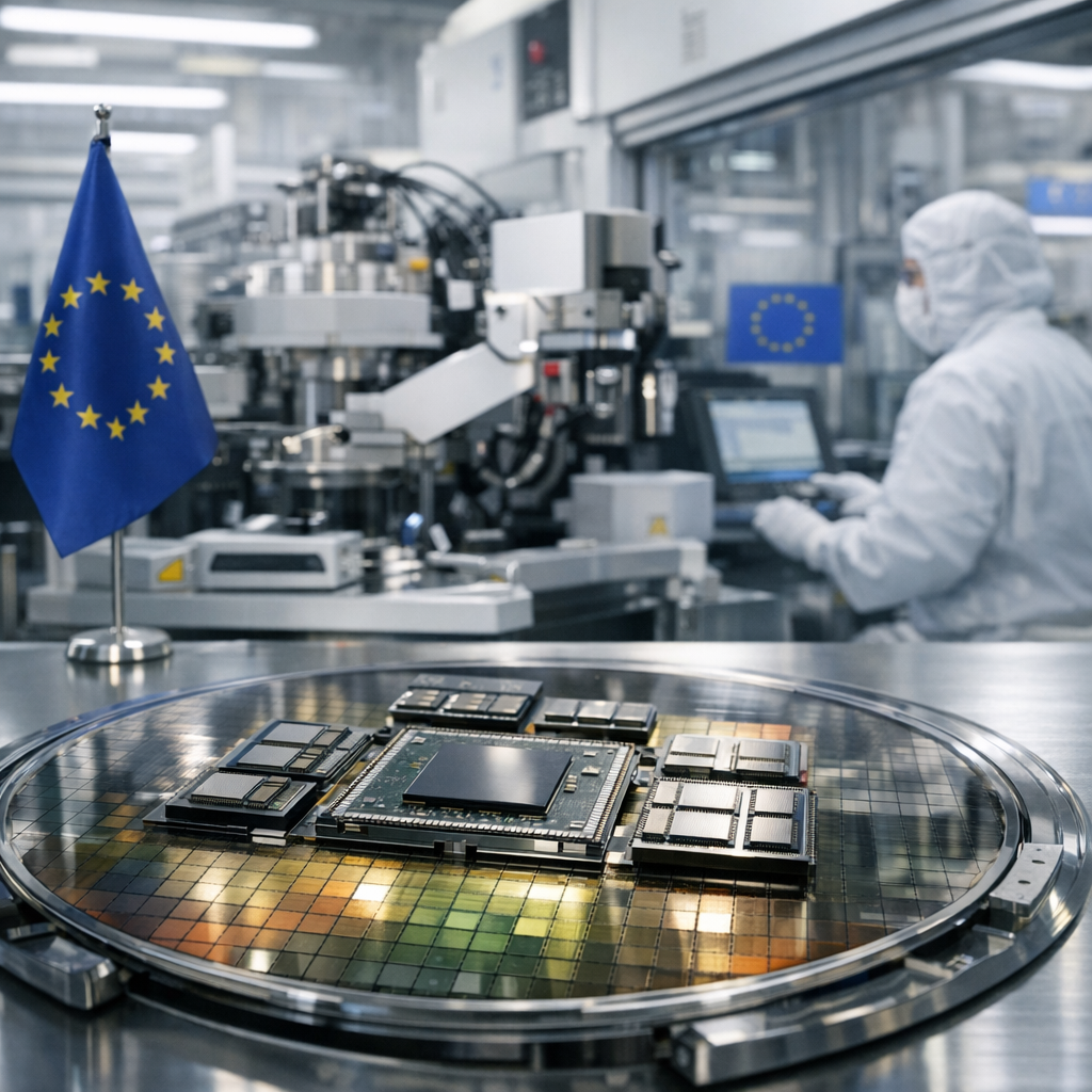
The European Commission has granted “Open EU Foundry” status to an innovative chiplet development and manufacturing facility, a move designed to expand open access to advanced semiconductor technologies and strengthen Europe’s position in the global chip ecosystem.
The designation was announced by the European Commission on its Digital Strategy website in an article titled “Open EU Foundry status granted to innovative chiplet facility.” According to the Commission, the new status recognizes a facility that will provide companies, startups, and research organizations with broader access to advanced chiplet design, prototyping, and manufacturing capabilities within Europe.
Chiplets—small semiconductor components that can be combined to create complex integrated systems—are increasingly seen as a strategic alternative to traditional monolithic chip manufacturing. By enabling modular chip design, chiplet architectures can improve performance, flexibility, and cost efficiency while helping overcome the technical and economic limits associated with producing ever more complex single-piece chips.
The European Commission said the Open EU Foundry designation is intended to promote a more accessible and collaborative semiconductor innovation environment. Facilities with this status are expected to operate with open access principles, allowing a wide range of users to develop and test semiconductor technologies using advanced infrastructure that would otherwise be out of reach for many smaller companies or research groups.
The new chiplet-focused facility will support research, prototyping, and early-stage manufacturing for next-generation semiconductor systems. By making these capabilities available to a broad community of developers, the Commission hopes to accelerate innovation in areas such as high-performance computing, automotive electronics, telecommunications, and artificial intelligence applications.
The initiative forms part of the broader implementation of the EU Chips Act, a policy framework designed to reinforce Europe’s semiconductor industry and reduce dependence on external suppliers. European policymakers have identified advanced packaging and chiplet integration as key technological areas where Europe can build competitive strengths within the global semiconductor value chain.
According to the Commission, making advanced fabrication infrastructure more accessible is essential for nurturing new ideas and enabling startups and smaller firms to move more rapidly from concept to testing and production. The Open EU Foundry framework aims to connect research facilities, industrial players, and emerging companies, creating a more integrated development pathway for semiconductor technologies.
Officials also emphasized the importance of collaboration across Europe’s semiconductor ecosystem. By opening specialized facilities to a wider group of users, the program seeks to ensure that knowledge, tools, and manufacturing capabilities are shared across borders and sectors, helping European innovators bring new chip architectures to market faster.
The Commission views chiplet technology as a particularly promising area for advancing this collaborative approach. Because chiplet-based systems can combine components built with different technologies and manufacturing processes, they offer a flexible route to creating powerful computing platforms without relying exclusively on the most advanced semiconductor nodes.
The granting of Open EU Foundry status therefore marks not only recognition of a specific facility but also progress in implementing a more open and distributed semiconductor innovation infrastructure across the European Union.
Through initiatives like this, EU officials aim to support the development of cutting-edge chip design and manufacturing capabilities inside Europe, strengthen industrial resilience, and foster an environment in which researchers, startups, and established companies can jointly develop the semiconductor technologies that will underpin future digital systems.