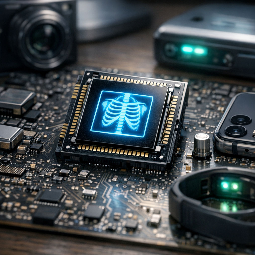
Researchers are pushing the boundaries of electronic sensing with a new class of semiconductor technology capable of detecting forms of radiation beyond the visible spectrum, according to a report published by Tech Xplore titled “X-ray vision for electronics: Scientists develop new chips.”
The work centers on advanced chip designs that can directly sense high-energy radiation such as X-rays, a capability traditionally confined to bulky and specialized detectors. By integrating this functionality into compact semiconductor devices, scientists aim to open the door to a range of applications, from medical imaging and industrial inspection to security screening and scientific instrumentation.
At the heart of the development is a rethinking of how standard electronic materials interact with high-energy photons. Conventional silicon-based chips are highly effective for visible light and everyday electronic processing but are less efficient when it comes to detecting X-rays. The researchers addressed this limitation by exploring alternative semiconductor materials and novel architectures that enhance sensitivity to higher-energy radiation while maintaining compatibility with established chip fabrication methods.
One of the key advances described involves improving how incoming radiation is converted into readable electrical signals. By optimizing the internal structure of the chip, the team increased the probability that incoming X-rays would generate measurable charge, reducing noise and improving resolution. The result is a device that can capture more detailed information about the radiation it detects, potentially leading to sharper imaging and more precise measurements.
The implications for healthcare are significant. Current medical imaging systems often rely on large, expensive detectors that can limit accessibility and portability. Compact, chip-scale X-ray sensors could lead to lighter, more affordable imaging devices, expanding their use in clinics, emergency settings, and remote locations. Similar benefits could extend to industrial environments, where portable inspection tools could improve quality control and safety monitoring.
Security and scientific research may also benefit. Enhanced detectors could improve the ability to identify hidden materials or structural defects, while in laboratory settings, more sensitive instruments could enable new experiments in physics, materials science, and biology.
Despite the promise, challenges remain before widespread deployment becomes feasible. Manufacturing scalability, long-term durability under repeated radiation exposure, and integration with existing electronic systems will need to be addressed. Researchers are also working to balance sensitivity with energy efficiency, ensuring that the chips can operate effectively without excessive power consumption.
Still, the development marks a notable step toward embedding advanced sensing capabilities directly into everyday electronics. As the Tech Xplore report makes clear, the convergence of materials science and semiconductor engineering is steadily expanding what chips can perceive, bringing technologies once confined to specialized equipment closer to mainstream use.