A growing bottleneck in the global semiconductor supply chain is pushing chipmakers to rethink a long-neglected step in production: advanced packaging. As traditional transistor scaling slows and the cost of building ever more sophisticated fabrication plants rises, the industry is leaning harder on packaging technologies that can boost performance, reduce power consumption and enable new chip designs by combining multiple components into a single module. That shift, described in the Globes article “Chip Industry’s Headache Is This Israeli Company’s Opportunity,” is reshaping investment priorities and opening doors for specialized firms that address the constraints of packaging capacity and yield.
For years, the economic center of gravity in semiconductors sat firmly in wafer fabrication, with the most valuable breakthroughs tied to smaller process nodes. Packaging was often treated as a downstream, lower-margin activity. Now it is increasingly a differentiator. Products built around chiplets, stacked memory and high-bandwidth interconnects are placing new demands on how chips are assembled, tested and integrated. Those demands are straining a market that already suffers from uneven global capacity, long qualification cycles and heavy dependence on a handful of Asian contractors.
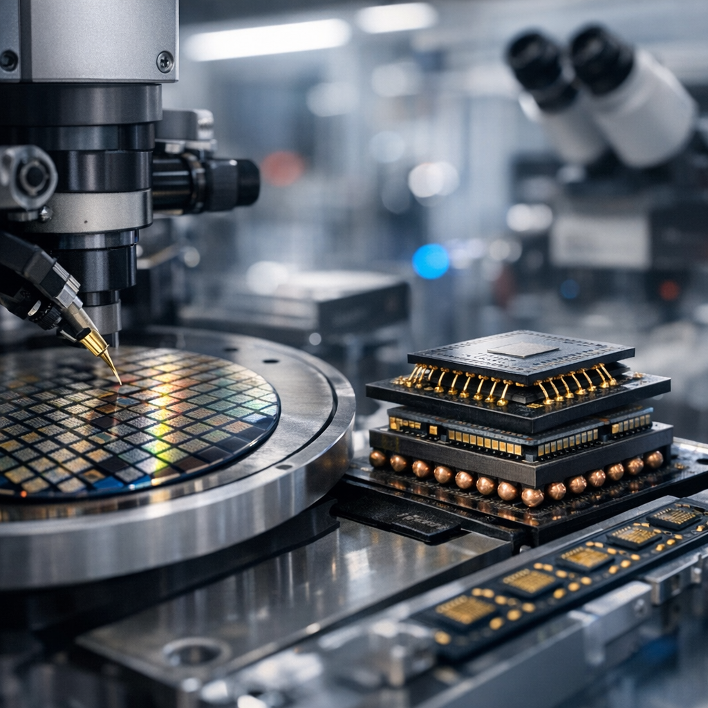
The Globes report frames this strain as a “headache” for the industry: advanced packaging is becoming a gating factor for bringing high-end processors to market, particularly for data centers and artificial intelligence workloads. While foundries expand, the supporting ecosystem for packaging and assembly is not scaling as quickly, and the technologies involved are becoming more complex. Moving to denser interconnects and multi-die architectures can introduce new failure modes, reduce yields and lengthen development timelines. For companies racing to meet demand, especially in fast-moving AI segments, delays or quality issues in packaging can blunt the advantage of leading-edge designs.
Against that backdrop, Globes highlights an Israeli company positioning itself as a beneficiary of the new emphasis on packaging. The company’s opportunity, as presented in the article, stems from offering tools and capabilities that help chipmakers and subcontractors raise yields and manage the finer tolerances of advanced packaging processes. As packaging steps become more intricate, the ability to detect defects earlier, measure critical parameters more precisely and optimize processes becomes more valuable. The broader implication is that value in semiconductors is migrating toward previously underappreciated parts of the production chain, where a single improvement in reliability or throughput can translate into meaningful savings.
Industry executives and analysts have increasingly described advanced packaging as the “new front line” of competition, not only technologically but geopolitically. Governments in the United States and Europe are subsidizing semiconductor manufacturing to reduce reliance on overseas capacity, yet packaging remains heavily concentrated in Asia. Rebalancing that footprint is difficult: packaging facilities are cheaper than cutting-edge fabs, but they require specialized know-how, sophisticated equipment and close collaboration with designers and foundries. Even when money is available, building an ecosystem takes time, and qualification by major customers can stretch over multiple product cycles.
The shift also reflects a deeper technical reality. The era when performance gains came primarily from shrinking transistors is giving way to an era of system-level engineering. Combining different process technologies in one package allows designers to use the best node for each function, improving cost and power efficiency. But the more heterogenous the package, the more critical the assembly and interconnect steps become. Thermal management, signal integrity and mechanical stress must all be handled within tighter limits, and testing becomes more difficult when multiple dies interact in complex ways.
In that environment, companies that supply inspection, metrology, process control and related solutions can find themselves in a strong position, provided they can prove their tools deliver measurable improvements at scale. The Globes article underscores that point by linking the industry’s packaging constraints with the prospects of an Israeli firm seeking to capitalize on the structural shift. The near-term story is about relieving a bottleneck; the longer-term story is about the industry’s evolving definition of what constitutes a “leading-edge” semiconductor product.
For chipmakers, the implications are immediate. As demand for advanced processors continues, particularly from AI infrastructure spending, the ability to secure packaging capacity and maintain high yields will influence product schedules and competitiveness. For suppliers, the opportunity is paired with pressure: customers will demand rapid integration into production lines, robust support and continuous innovation as packaging transitions advance quickly. For investors and policymakers, the message is that the semiconductor value chain is changing, and that strategic resilience depends not only on fabs but also on the less visible technologies that turn wafers into working systems.
The packaging crunch is unlikely to disappear soon. Capacity expansions take time, and the underlying trend toward multi-die architectures is accelerating, not slowing. If there is an opening for nimble, highly specialized firms, as Globes argues in “Chip Industry’s Headache Is This Israeli Company’s Opportunity,” it is because the industry’s next gains are increasingly won not just by making chips smaller, but by assembling them smarter.