New research is challenging long-held assumptions about how electrons move through metals, suggesting that copper—one of the most widely used conductors in modern electronics—may be capable of supporting ballistic electron transport under conditions previously thought impractical.
According to the article “Copper made ultra thin to reveal ballistic electron transport” published by Tech Xplore, scientists have observed electrons traveling through exceptionally thin layers of copper with minimal scattering, a behavior known as ballistic transport. In conventional conductors, electrons frequently collide with impurities, lattice vibrations, and other electrons, leading to resistance and energy loss. Ballistic transport, by contrast, allows electrons to traverse a material with far fewer disruptions, potentially enabling faster and more energy-efficient electronic devices.
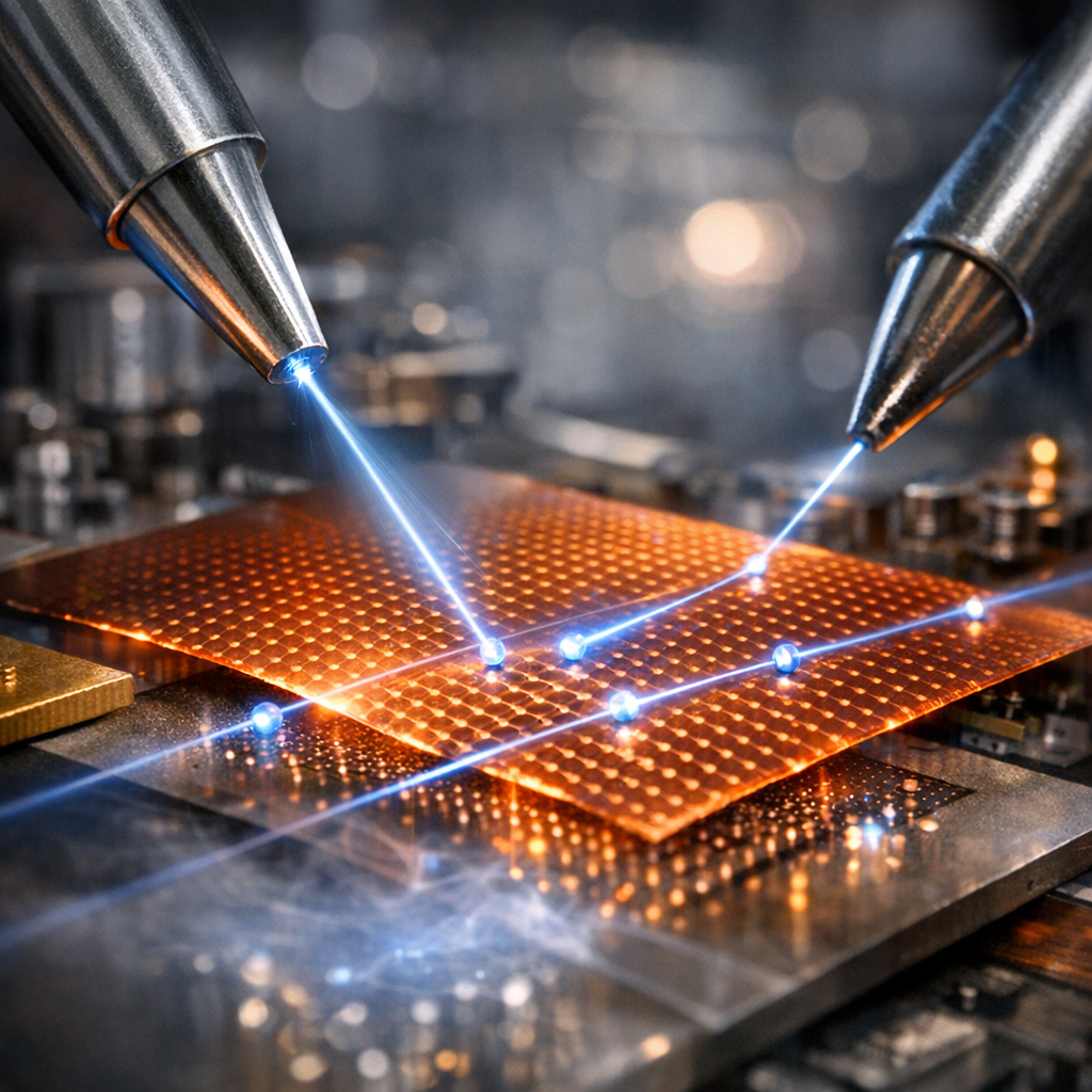
The findings hinge on engineering copper films at nanometer-scale thicknesses, where quantum effects begin to dominate electron behavior. By reducing the material to such extreme thinness and carefully controlling its structural quality, researchers were able to observe electrons moving across the copper layers in a near-collisionless manner over measurable distances.
This is notable because ballistic transport is typically associated with exotic materials or conditions, such as very low temperatures or specialized semiconductors like graphene. Copper, in contrast, is abundant, inexpensive, and deeply embedded in existing manufacturing infrastructure. Demonstrating ballistic behavior in such a familiar material could therefore have significant practical implications.
The researchers reported that when copper films are fabricated with exceptionally smooth surfaces and minimal defects, electron scattering is dramatically reduced. Under these conditions, electrons maintain their momentum over longer distances than expected, effectively behaving more like particles in a vacuum than in a conventional metal lattice.
If the phenomenon can be reliably reproduced and scaled, it could influence the design of next-generation microchips. As electronic components continue to shrink, resistance and heat generation in metal interconnects have become major bottlenecks. Ballistic transport in copper could help mitigate these issues by reducing energy losses and enabling faster signal transmission between transistors.
However, significant challenges remain before such effects can be translated into commercial technologies. Maintaining the precise structural conditions required for ballistic transport at scale, especially within the complex architecture of modern integrated circuits, is nontrivial. Even minor imperfections in thin films can reintroduce scattering and negate the effect.
Moreover, the distances over which ballistic transport has been observed are still relatively small, raising questions about how impactful the phenomenon can be in real-world devices where signals must traverse longer pathways. Researchers will need to determine whether the effect can be extended or integrated into hybrid systems that combine ballistic and conventional conduction.
Despite these hurdles, the work opens a new line of inquiry into how classical materials behave at the nanoscale. It suggests that, with sufficient control over structure and thickness, even well-understood metals like copper may exhibit properties typically reserved for more novel materials.
The study also underscores a broader trend in electronics research: revisiting established materials with advanced fabrication techniques to uncover previously hidden behaviors. Rather than relying solely on new compounds, scientists are increasingly finding ways to push familiar materials into regimes where quantum effects offer new functionality.
As semiconductor manufacturers confront the physical limits of current technologies, such insights could prove valuable. Whether ballistic transport in copper becomes a cornerstone of future electronics or remains a laboratory curiosity will depend on the ability to integrate these findings into scalable, reliable systems.
For now, the results reported in Tech Xplore point to a compelling possibility: that one of the oldest and most ubiquitous materials in electronics may still have untapped potential at the smallest scales.