Camtek, an Israeli maker of inspection and metrology tools for semiconductor manufacturing, is drawing renewed attention after a recent report highlighted the company’s performance and outlook. The April 15 article “Camtek 7” published by TechTime.news described the firm as benefiting from continued demand in advanced chip packaging and underscored investor focus on whether the current growth cycle can be sustained.
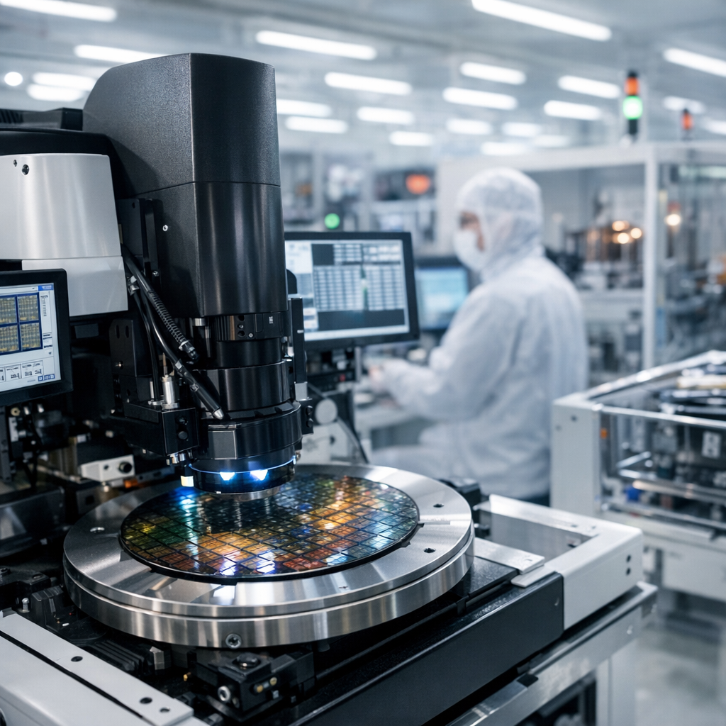
Camtek’s business sits in a crucial part of the semiconductor value chain: identifying defects and measuring critical dimensions during production, particularly in advanced packaging processes that combine multiple chips into a single high-performance module. As chipmakers and packaging houses push toward higher bandwidth and lower power consumption for data centers and AI-related workloads, inspection requirements have become more demanding, elevating the importance of equipment suppliers that can deliver higher precision and throughput.
The TechTime.news piece pointed to momentum in areas such as heterogeneous integration and other packaging approaches where tighter tolerances increase the need for sophisticated metrology. That emphasis reflects a broader industry shift. While leading-edge wafer fabrication remains the headline driver of semiconductor investment, many of the most significant performance gains in recent years have come from how chips are assembled and interconnected. This redistribution of innovation dollars has helped expand the addressable market for suppliers focused on packaging-related inspection.
Investors are also weighing how resilient Camtek’s growth will be against the semiconductor industry’s cyclical tendencies. Demand for capital equipment can be volatile, shaped by swings in end markets such as consumer electronics, industrial systems, and communications infrastructure. The current cycle, however, is being propelled by large-scale data center spending and AI acceleration, and that in turn is reinforcing investment in advanced packaging capacity. For companies like Camtek, the key question is whether that buildout translates into multi-year equipment utilization and repeat orders, or whether it tapers once initial expansion targets are met.
Competition is another central issue. Inspection and metrology is a high-stakes segment with entrenched global players and a fast pace of technical change. To maintain its position, Camtek must keep pace with evolving packaging architectures, new materials, and increasingly complex quality requirements, while also ensuring installations, service, and support at large manufacturing customers are executed reliably. In this environment, operational performance can influence customer standardization decisions that determine procurement for years.
The TechTime.news article framed Camtek’s story as one of continued opportunity tied to structural trends in chip production. The company’s trajectory will likely remain closely linked to how quickly advanced packaging becomes the default pathway for performance improvements across major semiconductor categories, and how effectively equipment suppliers can meet the resulting demands for higher accuracy, automation, and process control.