A new generation of semiconductor technology may be poised to redefine how electronic devices handle multiple tasks simultaneously, according to recent reporting by TechXplore in its article “Semiconductors for the multi-tasking era: A new type of device.”
The report highlights research into advanced semiconductor architectures designed to overcome long-standing limitations in traditional computing systems. Conventional chips process tasks in largely sequential or compartmentalized ways, often requiring significant energy and time when switching between operations. The emerging approach described by researchers aims to integrate multiple functions more fluidly within a single device, enabling more efficient multitasking without the usual trade-offs in speed or power consumption.
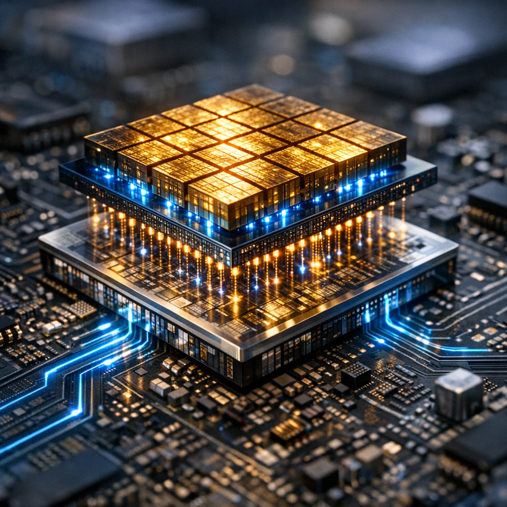
At the center of this development is a novel device concept that blends memory and processing capabilities, reducing the need to shuttle data back and forth between separate components. This shift addresses one of the most persistent bottlenecks in modern computing—often referred to as the Von Neumann bottleneck—where data transfer between memory and processors can slow performance and increase energy demands. By embedding these capabilities together, the new technology could allow systems to handle complex, parallel workloads more seamlessly.
Researchers involved in the work suggest that such devices could have significant implications for artificial intelligence, edge computing, and mobile technologies, where rapid decision-making and energy efficiency are critical. For AI applications in particular, the ability to process large volumes of data simultaneously while minimizing latency could lead to more responsive and capable systems, from autonomous vehicles to real-time language processing tools.
The innovation also reflects a broader trend in semiconductor research, as engineers look beyond traditional scaling—shrinking transistors to pack more onto a chip—and instead focus on new materials and architectures. This includes exploring neuromorphic computing approaches that mimic aspects of neural processing, enabling systems to handle multiple streams of information in ways that resemble human cognition more closely than conventional binary logic.
While the technology remains in the research stage, the implications outlined in TechXplore’s coverage point to a potentially transformative shift in chip design. If successfully commercialized, these multitasking semiconductors could help meet growing demands for faster, more efficient computing across industries, from consumer electronics to advanced scientific applications.
As the limits of existing semiconductor approaches become more apparent, innovations like these underscore a critical pivot in the field—one that prioritizes adaptability and integrated functionality over sheer transistor density. The coming years will determine whether such concepts can move from laboratory prototypes to the foundation of next-generation computing systems.